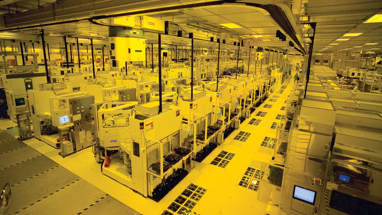
The semiconductor manufacturing process has long been noted to be lengthy, complex, and expensive, and because of this, process control tools have seen a growing impact. In 2024, while wafer front end sales increased by 6-8%, process control had outsized growth of 12%. In the future, this trend will likely continue – especially as the process node size shrinks. So why is process control so critical?
Process control finds errors and boosts the yield in manufacturing processes. In chipmaking, this process is photolithography. Photolithography is highly complex: it entails projecting patterned light onto silicon to build transistors and other structures. The patterns are referred to as photomasks. Through a series of light exposures and chemical applications, structures as small as tens of nanometers can be created. But because of this extreme scale, every aspect of the system must be flawless: the design, the photomasks, the lens and mirrors, and the silicon itself.
Before making the chips, though, the photomask set first has to be created. These serve as the templates for each chip layer, and they must be perfect. And, there isn’t just one photomask per chip – some chips require a set of upwards of 50, and whole sets are valued at tens of millions of dollars. Upon manufacturing these sets, they must be defect-free to avoid introducing printed defects. These sets are reused many times, so ensuring these are clean, particle-free, and unaltered for each new iteration is extremely important, especially with the next-generation EUV systems, which are inherently powerful and produce tin particles. There are many places where this process can fail, and it’s important to validate at each potential point of failure. Process control can aid in this by both finding defective designs and measuring structures to confirm that all photomasks are made to exact specification.
Then, when making the chips themselves, many other issues can arise due to the complexity and required precision. They can range from CAD design and modeling issues to small particle contamination to optical abnormalities. Additionally, slight tool drift, or changes in system properties such as mirror and lens arrangements, can cause printing issues. Some errors can result in more loss than others, but each wafer lost costs about $20,000, not to mention time on the scanner and space in the cleanroom. If defects can be caught with process control tools, the manufacturing process can be refined to significantly improve yield.
Without process control, chipmakers like TSMC, Samsung, and Intel, would struggle to produce profits. The complicated nature of manufacturing, along with the high cost tools and substrates, would be impossible to justify without strong yields, making process control indispensable. Why has process control seen outsized growth? It seems as though today’s advanced chip manufacturing will require even more attention to detail than previous generations of chips. And looking to the future, as we get to Angstrom-level process nodes, process control will grow more vital, where a single misplaced atom can become a critical defect.
Thanks to Vijay Ramachandran for reading drafts of this.